Deploying Xilinx Zynq UltraScale+ RFSoC
Xilinx Zynq ULtraScale+ RFSoC is changing the way engineers can design and package small, high channel count systems. This technology not only offers new possibilities for 5G applications, but has significant impact in military and scientific systems, justifying the claim in Xilinx’s announcement that “Xilinx Unveils Disruptive Integration and Architectural Breakthrough for 5G Wireless with RF-Class Analog Technology.”
To get better appreciation of the capabilities of RFSoC and understand how to best use the advantages of this technology, it’s worth taking a quick look at current trends in data converters and signal processing.
What is RFSoC?
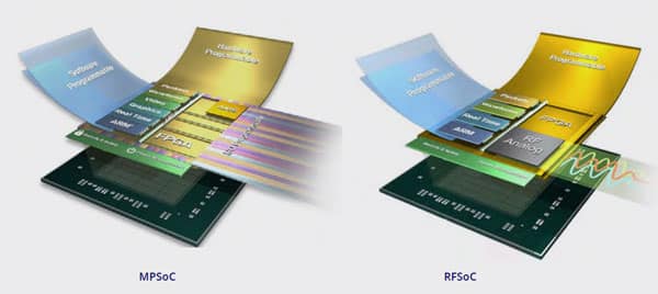
RFSoC or more properly, Zynq® UltraScale+™ RFSoC is based on Xilinx’s prior family, the Zynq UltraScale+ MPSoC. The MPSoC is a system on chip architecture that includes up to four ARM Cortex-A53 application processors and two ARM Cortex-R5 real-time processors integrated into the UltraScale+ programmable logic. This solution offers the software programmability and flexibility of a processor with the hardware programmability and performance of an FPGA in a single IC.
RFSoC builds on the MPSoC foundation and adds eight 5 GSPS 14-bit A/Ds each equipped with programmable Digital Downconverts (DDC) and eight 10 GSPS 14-bit D/As each equipped with Digital Upconverters (DUC). While other A/D and D/A configurations are available, we’ll consider the eight A/D and eight D/A configuration for the rest of this paper. Below is an image that shows the similarity between the MPSoC and RFSoC.
Improvements in SWaP and Cost
A common term in military applications is SWaP, which stands for Size, Weight and Power and refers to the ongoing requirement to reduce these attributes for communications, reconnaissance, radar and various types of signal acquisition and processing systems. The need for smaller, lighter and less power becomes obvious when you think about where these systems are often deployed. Unmanned vehicles like unmanned aerial vehicles (UAV) and unmanned underwater vehicles (UUV) frequently require stealth to achieve their mission. Smaller, lighter and less power usually equates to stealthier, enabling these systems to be more effective.
Manpack (or womanpack) systems where the communications or direction finding equipment and associated power supply are worn by personnel are another target for SWaP reduction. Here again, smaller, lighter and less power is needed for making a practical, human carried system.
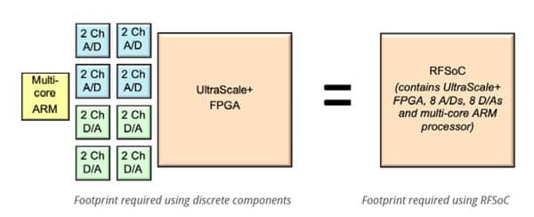
RFSoC’s high level of integration provides a significant amount of SWaP reduction when compared to designing the same functionality with discrete components. The example below shows the reduction in size by representing component footprints graphically. In the comparison, each component is roughly to scale, and space has been left between the discrete components to model a typical PCB layout, where ICs need space between them for assembly and placement of passive components. The RFSoC implementation can save 50% or more in overall size compared to the discrete approach.
While RFSoC can reduce weight at the component level, that savings is minimal when you consider the total weight of nine ICs compared to a single RFSoC. Where weight savings can be appreciated is when you look at power. For every watt of power in a system, comes the weight of a cooling solution, either in metal or composite heatsinks, or in some systems, more exotic solutions like liquid and vapor cooling. RFSoC can easily bring power savings of 30%-40% or more compared to typical discrete solutions reducing the cooling solution complexity and weight. And in portable systems, every watt that can be eliminated results in smaller, lighter batteries and longer operation time.
A key reason for the reduced power of RFSoC is the elimination of the interfaces needed to connect the various ICs in a discrete solution. Most data converters sampling at 1 or 2 GHz or higher depend on serial interfaces to move digital data between the converter and the FPGA. These interfaces expend power at both the data converter side and the FPGA side in serializing and deserializing (SerDes) circuitry. The most common serial interface protocol used for converters is JESD204. By integrating the converters directly into the FPGA, the serial interfaces are eliminated as well as data transfer latency which the SerDes process and protocol introduce. (More on serial vs. parallel converter interfaces and latency later in this paper)
Another parameter often tacked on to SWaP is cost, sometimes referred to as SWaP-C. Here again RFSoC address the requirement. The same comparison used earlier of implementing the functions of the RFSoC as discrete components yields the following results:
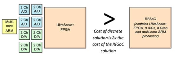
The cost of a typical multi-core ARM processor + (4 x Dual 5 GSPS A/Ds) + (4 x Dual 10 GSPS D/As) + Kintex™ UltraScale+ FPGA (with equivalent programmable logic and DSP density of the RFSoC) = approximately 2x the cost of the same functionality delivered in a single RFSoC.
While savings at any level is always welcome, the real benefit of the reduced cost can be seen in systems where many channels of A/Ds and D/As are required. Massive multiple-input multipleoutput (MIMO) antennas are being targeted for applications from Wi-Fi to LTE to 5G. Massive MIMO antennas typically start at 8×8 configurations (8 receive channels and 8 transmit channels) and can be multiples of that configuration. This is a perfect match for the converters in the RFSoC.
Another high channel count application is phased array radar. The Multi-function Phased Array Radar (MPAR) initiative combines the functions of several national radar networks into a single system for aircraft and weather surveillance. It is not uncommon for these antenna arrays to be specified with 64 or more elements, with each element requiring an A/D and D/A pair combined with signal generation and receive and control processing. With these systems as well as military surveillance and targeting systems where hundreds of elements can be required, the savings found in RFSoC’s integrated solution can add up quickly.
Data Converter Interfaces
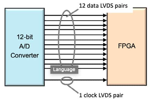
Up to this point the advantages of RFSoC have been primarily in improving on already available solutions, saving on size, weight, power and cost compared to discrete component solutions. But by integrating the data converters into the FPGA, RFSoC offers a solution that is currently unavailable using existing technology. To understand this you must first look at how data converters connect to FPGAs. Using A/Ds as an example (but this is the same for D/As), connecting a 12-bit A/D to an FPGA using a parallel interface might look like this where each bit is represented by an LVDS pair and an additional pair is used for data ready or clock.
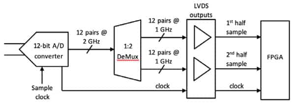
In some cases the interface can make use of double data rate (DDR) technology where data is transferred on the rising and falling edge of the clock, effectively doubling the amount of data transferred in a single clock cycle. But even with DDR, parallel converter interfaces become problematic for data converters with sample rates above about 1.5 GHz due to the speed limitations of the LVDS interfaces on FPGAs. One solution to overcome this is to use a 1:2 demultiplexed interface (DeMux) where data is sent over two parallel interfaces each running at half of the sample rate. In the 12-bit A/D converter example, if the converter is sampling at 2 GHz, each of the 12-bit paths following the DeMux are running at 1 GHz. This keeps each 12-bit interface below the maximum clock rate allowed by the FPGA LVDS interface but still delivers the data needed to support the 2 GHz sample rate.
But this solution also becomes problematic at higher speeds. Using this same technique, a 4 GHz A/D would require a 1:4 DeMux. This quickly starts to become a PCB design challenge when you consider the number of pairs needed and that these signals need to be critically routed to maintain tight length matching between pairs so data arrives at the FPGA across all 12 bits at the same time. In addition to the routing challenge, a 12-bit A/D converter now requires 4 sets of 12 pairs (or 96 individual I/O pins, not including clock pins) to interface to the FPGA. In a typical FPGA device where 400 to 600 I/O pins might be available for interfacing all parallel devices like A/D and D/A converters and memory, half the pins could easily be used to connect just two 4 GHz A/D converters.
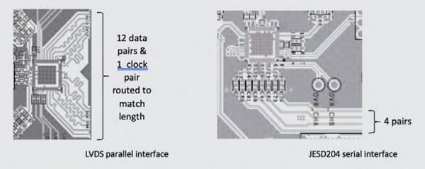
An alternate solution to the high-pin count interface is to use a serial interface to connect data converters. JESD204 was created for this exact purpose. JESD204 makes use of the FPGA gigabit serial interfaces instead of LVDS. The example below shows a PCB routed for a 1 GHz 12-bit A/D connected via parallel LVDS and a PCB routed for a similar 1 GHz 12-bit A/D connected via four high speed serial interfaces (or lanes) using JEDS204. The four lanes pose less of a PCB design challenge because of the reduced number of signals as well as the fact that the interface standard includes clock and data recovery features which eliminate the need to critically match the length of all lanes.
So while JESD204 can be a good solution for many high speed data converter applications, it’s not a perfect solution. The JESD204 IP and gigabit serial interface add about 1W to the power budget for every four lanes used. JESD204 is a proprietary IP core and typically requires a paid license to use it. In addition, using JESD204 can add complexity to the FPGA IP design. In applications where multiple converters across multiple ICs need to be synchronized, JESD204 requires a more elaborate clocking solution than parallel interfaces adding some additional circuitry and complexity. But while each of these obstacles can add power, cost, complexity and increased size, none is typically a showstopper.
Where JESD204 becomes a true impediment for some applications is in link latency. Where a parallel converter interface can delay the data by at most a few sample clock cycles for local buffering, the JESD204 protocol and the SerDes required to support it can add 80 sample clock cycles or more of latency from when the data is converted to when it is available in the FPGA for an A/D converter and in the reverse direction for a D/A converter. In some applications where data is streamed and processing results are not required in real-time, this poses no problem. As long as the data arrives at the FPGA without losing any samples, how long it takes to get there is not critical. But in many applications including high-speed tight control loop systems, some radar systems, and electronic warfare like countermeasures, where there is a very short time allowed for acquiring the data, processing it and turning it around, this latency is a non-starter and eliminates JESD204 based solutions.
So, what does all this have to do with RFSoC? With the data converters integrated directly into the FPGA using parallel interfaces, they don’t require the prohibitively high pin count external connections needed for discrete parallel interface converters allowing more converter channels to be supported by a single FPGA. In addition, the latency associated with a JESD204 serial interface is not an issue. This makes RFSoC an attractive to solution for high channel count and low latency applications.
Hardware Design with RFSoC
The circuit density and small size of the RFSoC create some unique challenges for circuit and PCB designers when engineering systems using the FPGA. Designing and laying out the PCB for the analog interface containing 16 channels (8 A/D and 8 D/A), requires attention to even the smallest details, to maintain signal quality and reduce crosstalk in such a dense configuration. Similarly, the RFSoCs GTYs (gigabit serial interfaces) are capable of running at higher than 32 Gb/sec. This poses another layout and routing challenge to the PCB design to maintain these speeds with signal integrity. For some operating modes, the RFSoC requires up to nine different supply voltages. Add to that another four or five supplies for peripheral circuitry and the power generation and management design can become complex very quickly. While each of these challenges can be demanding on their own, consider that many of the applications where RFSoC can bring the greatest benefit are in space restricted and harsh environments, exacerbating the design challenge.
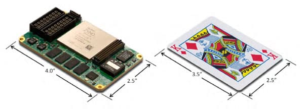
Mercury Systems® has taken a unique approach to delivering RFSoC functionality to our customers. Our QuartzXM™ eXpress Module is a small 2.5” x 4” board containing the Zynq UltraScale+ RFSoC FPGA and all peripheral and power circuitry needed for support and operation. The concept behind the QuartzXM is simple: to provide the RFSoC functionality in a small, fully designed package that can be used on different carriers as needed to match the specific interface requirements of different applications. By offering the RFSoC on the QuartzXM, Mercury Systems is delivering not only the RFSoC functionality, but is delivering a solution where many of the most demanding circuitry and packaging challenges have been solved.

Our Quartz™ line includes board products in standard form factors with 3U VPX, SOSA aligned 3U VPX, PCIe, SFF enclosure and SFF subsystems, delivering the QuartzXM in turn-key solutions ready for immediate deployment. The products are available in commercial and rugged, conduction cooled versions, and in many situations will be the final deployed solution. But with the modular design of QuartzXM, the standard form factor board can be the platform where the application is developed and proven, and then migrated to a custom carrier platform for deployment.
Software and IP Design
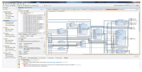
With each new family of FPGA, there has been a constant progression towards more powerful processing solutions. Each new family adds more logic density, faster logic fabric, more DSP resources, more on-chip memory, faster interface and now with RFSoC high sample rate A/D and D/A converters. While these new capabilities are certainly welcome, and they do enable more and more complex applications to be targeted at FPGAs, they also raise the bar for better and more capable design tools to handle the increasing complexity and size of the new IP that can be created. Xilinx has addressed the design tool challenge with their Vivado® Design Suite. It includes tools for every aspect of the design cycle. The latest version has improvements in performance with faster routing and more efficient FPGA resource usage allowing denser designs. Vivado also addresses the increasing design complexity challenges with tools for creating processing IP with C-language specification, an integrated software development kit that targets the ARM processors, and plug-and-play block diagram based IP integration with IP Integrator. While all of these tool improvements go a long way in enabling both software and IP engineers, the job of creating a complete system solution can be greatly accelerated when manufacturers of FPGA based hardware products provide IP and software libraries to support the specific features of the hardware. The better the manufacturer can provide a foundation of software and IP for the engineer to build their application on, the faster the engineer can complete the job of producing a final, robust system.
All Mercury Systems hardware products include a full suite of FPGA based functions allowing the product to be used immediately in a range of applications without the need to create any FPGA IP. For Sponsored by Strategies for Deploying Xilinx’s Zynq UltraScale+ RFSoC 11 all of our A/D or D/A based products the functions can include data acquisition and waveform generator engines, data tagging and metadata creation, VITA-49 packet creation, digital downconverters, multichannel and multi-board synchronization, optimized DMA for moving data on and off board through PCIe or 10GigE, in addition to IP targeted at specific applications.
RFSoC again brings new challenges and solutions with the sheer amount of data the A/D and D/A converters can introduce and the minimum latency interfaces between data converters and programmable logic in time critical applications. Mercury Systems’ Quartz products address some of the most common requirements of RFSoC targeted applications with new built-in IP ready to use with no additional IP design needed. These include an enhanced acquisition engine that supports the full bandwidth 4 GHz sample rate with options to snapshot data to on-board memory or to stream over dual 100 GigE interfaces, an optimized x16 decimator for data reduction in high channel count applications, and an enhanced waveform generator engine for outputting D/A data supplied by the 100 GigE interface or from waveforms loaded to on-board memory. In each case the installed functions can provide a final solution or be the basis of a custom solution when built upon using the Mercury Systems Navigator™ FPGA Design Kit (FDK).
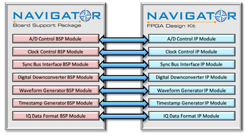
The Navigator FDK provides a library of all of Mercury Systems’ IP functions as blocks that can be used in Xilinx’s Vivado IP Integrator, giving the IP designer immediate access to the product’s entire FPGA design as a block diagram. Individual IP blocks can be removed, modified, or replaced with custom IP to meet the application’s processing requirements. If at any time a designer needs to work with the VHDL source code directly, it is always accessible in a source window, as well as full on-line documentation of every Mercury Systems IP core. Navigator FDK leverages the features of Vivado allowing an engineer to start designing with the FDK immediately without the need to learn new software tools and streamlines the path to a final application solution by providing the foundation for custom IP to be built on.
The companion product to the Mercury Systems Navigator FDK is the Navigator Board Support Package (BSP). With every creation of, or modification to an IP block, a change to software, most likely running on the RFSoC’s ARM processors, to control the new or modified IP might be needed. The Navigator BSP was designed to help manage this relationship between IP and software. The BSP provides C language functions and utilities structured to map the IP blocks provided in the FDK. This one-to-one relationship between IP and the software to control it is another path to manage the increasing complexity of applications.
RFSoC brings new possibilities for addressing some of the most challenging requirements of high bandwidth, high channel count systems. Understanding how this new technology can specifically address SWaP-C and low latency applications is key to matching it to many applications that can benefit from it the most. And while Xilinx has provided a rich set of tools, IP and support at the chip level, equipment manufactures like Mercury Systems, using RFSoC at the center of their board architecture, can leverage the power of RFSoC by providing unique solutions to streamline the path from RFSoC to a deployed system.
About Mercury Systems
Mercury is the leader in making trusted, secure mission-critical technologies profoundly more accessible to aerospace and defense.
Purpose. Innovation that Matters® By and For People Who Matter
Vision. Make the world a safer, more secure place for all. Our goal is to provide all processing solutions on every system requiring uncompromised computing.
We're Here to Help
Resources
Related Companies